
This blog is to introduce the HJ-840 SIP and its corresponding low cost evaluation board HJ-840 that can be used to develop the Nordic nRF52840 chipset. The HJ-840 is the qualified chipset on the Nordic Official Webpage. HJ-840 is the SIP package that integrates the antenna circuit and DCDC power supply inside the package. It is much easier for the software developer to build up their own PCBA instead of spending time to do the antenna matching and power regulator control. The cost of the HJ-840 EV is around ~USD $10.0 compared to the nRF52840 DK board ~USD $49. The HJ-840 EV board can work on all the Nordic nRF5 SDK.
https://www.nordicsemi.com/Nordic-Partners/3rd-party-modules

https://www.nordicsemi.com/News/2020/07/Tangshan-Hongjias-HJ840-SiP-module-employs-nRF52840-SoC
In this blog, I would provide guidelines on how to modify the nRF5 SDK and run it on the HJ-840 evaluation board.

Tangshan, China-based Tangshan Hongjia Electronic Technology Co., Ltd, has selected Nordic’s nRF52840 Bluetooth® 5.2/Bluetooth Low Energy (Bluetooth LE) advanced multiprotocol System-on-Chip (SoC) to provide the wireless connectivity for its ‘HJ-840’ ultra-compact System-in-Package (SiP) module.
Weighing only 0.3g, the HJ-840 SiP module comes in a 6.2mm * 7.0mm * 0.9mm package size and is designed for OEMs developing highly space-constrained applications, for example advanced wearables, miniaturized sensors, and medical devices. The SiP module features a built in long-distance, high-performance antenna, as well as support for an external antenna if required. According to the company the antenna and the Nordic SoC’s support for Bluetooth Long Range enables the module to achieve a range of between 50 and 80 meters in open areas (TX power 0dbm, 1Mbps throughput).
HJ-840 module features a built-in antenna, inductor, and RF matching circuits, and operates in low power DC/DC mode to minimize current consumption. The modules are designed for beacons, proximity, health and fitness, medical, and smart lock applications.
The benefits of SiP technology include achieving greater functionality in a reduced time-to-market window that cannot be accomplished through silicon integration or ASIC development. Other advantages include reduced board area, board layers, and costs.
Material of the HJ840 can be downloaded here.
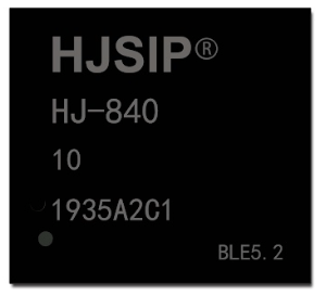
The features of HJ-840 are the following.
- 6.2mm * 7.0mm * 0.9mm
- Antenna inside the package
- Pad pitch: 0.65mm: Package: LGA64
- Operational Temperature Range : -40 to +105C
- GPIO pin: 48
- DCDC mode support
- Use internal RC for 32KHz operation
Datasheet of HJ-840 can be downloaded here.
Key Benefits on the HJ-840 SIP Module
Compared to the circuit configuration inside Nordic nRF52840 specification (No. 5 schematic), it can save the L2, L2 and the part of circuit components of the antenna.

HJ-840 Evaluation Board
- On-board 1.2V and 3.3V two-way voltage regulators can be used for low-voltage and high-voltage working mode related tests.
- On-board CH340 USB TO TTL, which can directly communicate with the computer
- All IOs are led out through 2.54mm pin headers.
Order the HJ-840 EV board can be gone through https://tshjdz.en.alibaba.com/.
Schematic of the HJ-840 Evaluation Board
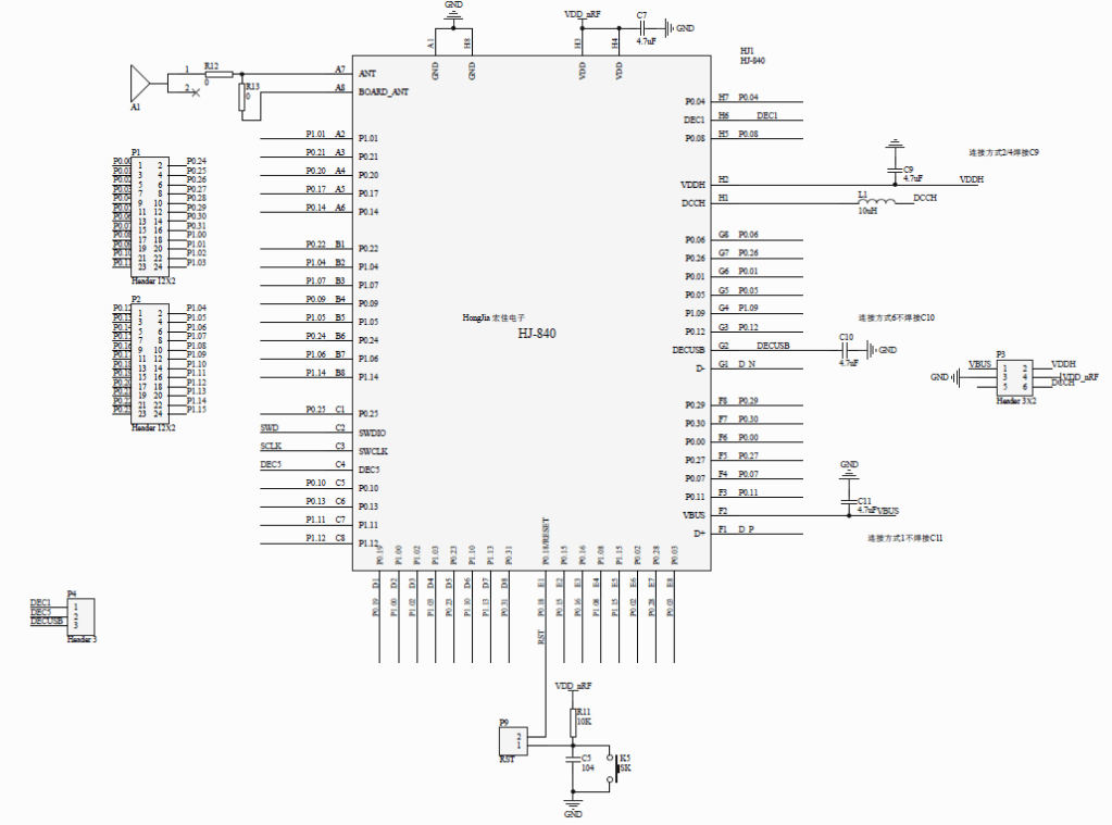

How to connect the JLInk for programming
The HJ-840 EVB is equipped with a jumper set to connect the JLINK for programming and debugging. It needs to connect with the external JLink adaptor through 4 pins (SWDIO, SWCLK, VCC and GND).


Configuration on the nRF5 SDK to build with HJ-840 Evaluation Board
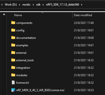
In this blog, I am using the Nordic nRF5 SDK 17.0 as the baseline. It should be very similar procedures to work on other nRF5 SDK and it can work on my github example also.
How to use the internal RC and DCDC for the BLE Application
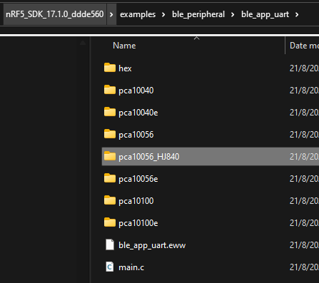
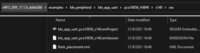
After you get the Nordic nRF5 SDK 17.1, we select the example\nRF5_SDK_17.1.0_ddde560\examples\ble_peripheral\ble_app_uart
Duplicate the pca10056 and create the new folder pca10056_HJ840
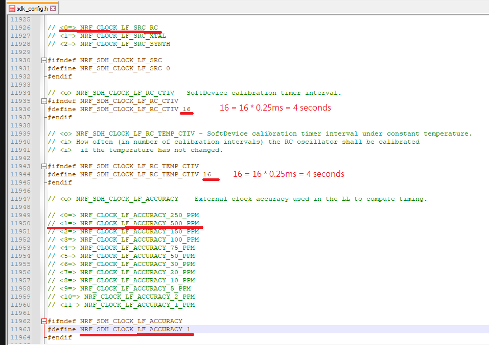
Use the internal RC instead of external 32kHz crystal (modify the sdk_config.h), more details can be found here.

New sdk_config.h to use the internal RC
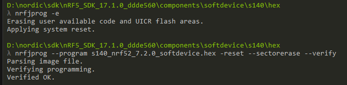
Download the Softdevice S140 on the command line
Open the project through Segger Embedded Studio
Enable the DCDC if using the BLE softdevice (more details)
    // Using the Low power mode
    err_code = sd_power_mode_set(NRF_POWER_MODE_LOWPWR);
    APP_ERROR_CHECK(err_code);

    // Enable the DCDC
    err_code = sd_power_dcdc_mode_set(NRF_POWER_DCDC_ENABLE);
    APP_ERROR_CHECK(err_code);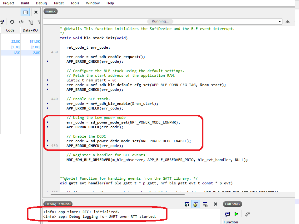
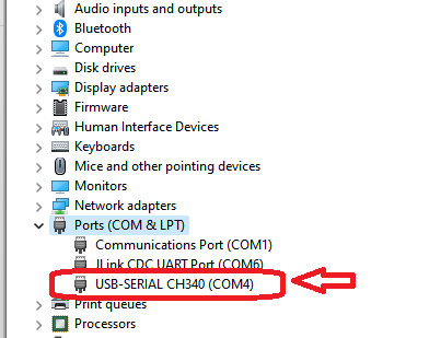
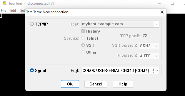
How to use the UART instead of the RTT (JLINK) to print out the log.
HJ-840 evaluation board has the CH340 (USB to UART adaptor) chipset. It can be used for the UART communication such as log print out.
Use the examples\ble_peripheral\ble_app_hrs\pca10056_HJ840\s140\ses and modify to use the internal RC instead of external 32kHz crystal.
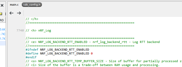
Disable the RTT Log inside the sdk_config.h
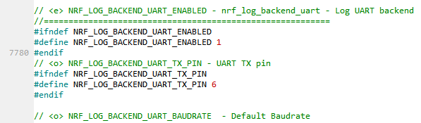
Disable the UART Log inside the sdk_config.h


If you are interested to evaluate the HJ-840 EV board or get the HJ840 SIP, you can visit the webpage http://hjsip.com.cn/.
You can also contact them as the below information.

Phone:+86-15833463803 or +86-18131562111
QQ:2436548842
Email:liyinfei@tshjdz.com or liujiahang@tshjdz.com or wujunwei@tshjdz.com
Address:Room 205, Block A, Hengda Technology Park, Ronghua West Road, Lubei High-tech Zone, Tangshan City, Hebei Province
Welcome to give any comments and suggestions on this blog.

Hello,
I have bought this development kit. It is a great product and I love it. I am facing issues with it nRFUSB. I am using example for USB console from nRF Connect SDK and it is working fine on nRF52840 DK but when I port it to this kit, nRFUSB does not appear in the device manager of my computer.
Please guide me what I am doing wrong.
Thanks
LikeLike
your email, is samawan@live.com?, right?
LikeLike
it is using the internal RC instead of external one.
you should configure and specify to use internal RC.
LikeLike