This blog describes how to use the SPI Master / Slave role on the nRF52 series.
In general, there are 4 connection wired on the SPI interface.
- Chip Select (CS)
- Clock (SCK)
- MOSI (Master Output Slave Input)
- MISO (Master Input Slave Output)
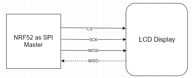
LCD Display Application
For the LCD display application, the nRF52 acts as the SPI master role and connects as below through SPI interface.
Case 1:
Case 2:

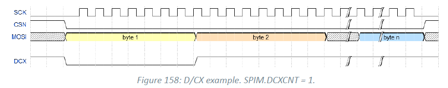
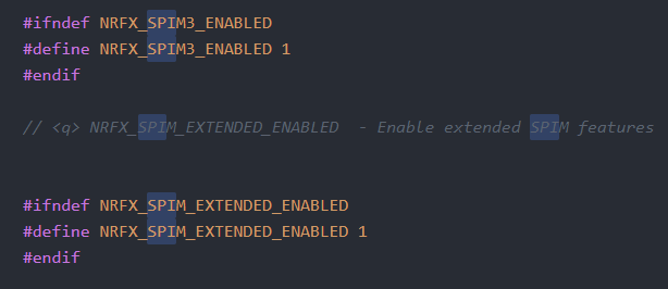
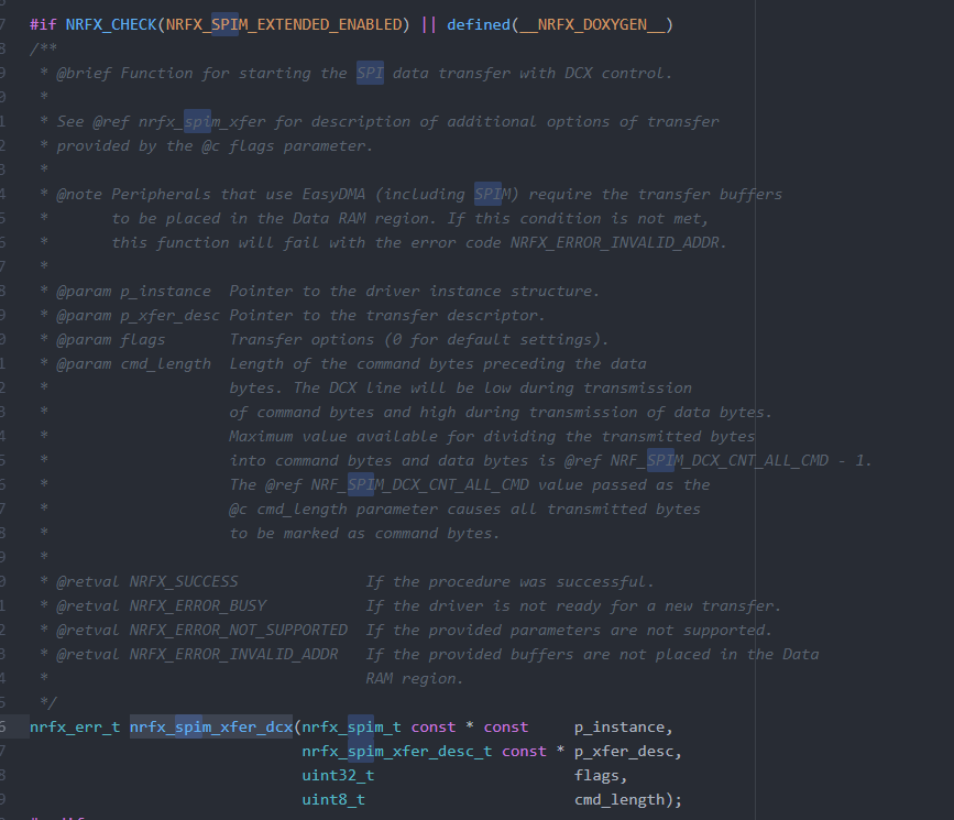
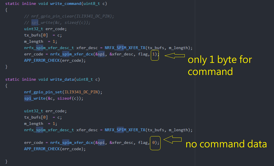
For the 2nd case, it has the additional DCX/DC pin for the LCD display. This pin is introduced on the NRF52840. (SPIM3 — high speed SPI bus). It can use to further improve the data transmission speed.
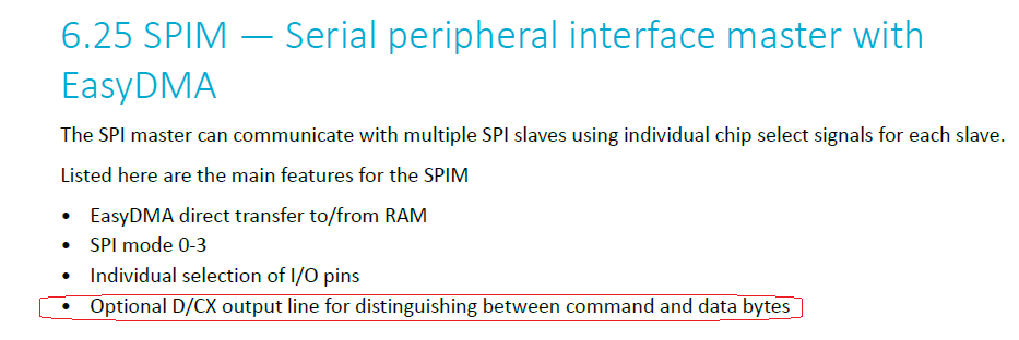
- DCX pin is low — command
- DCX pin is high — data
SPI driver (nrfx_spim)
Sensor Application
nRF52 series can act as the SPI master and SPI slave.
| nRF52810 | nRF52811 | nRF52832 | nRF52840 | |
| SPI Master (8MHz) | 1 | 2 | 3 | 3 |
| SPI Slave (8MHz) | 1 | 2 | 3 | 4 |
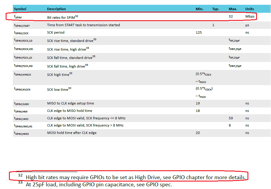
| SPI (32MHz) | x | x | x | 1 |
| QSPI | x | x | x | 1 |
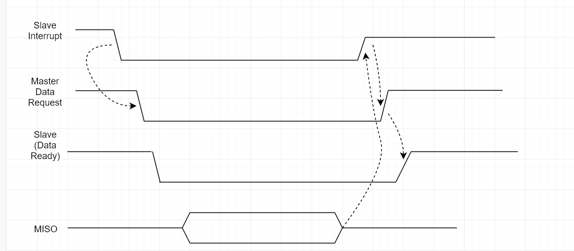
SPI Slave Mode
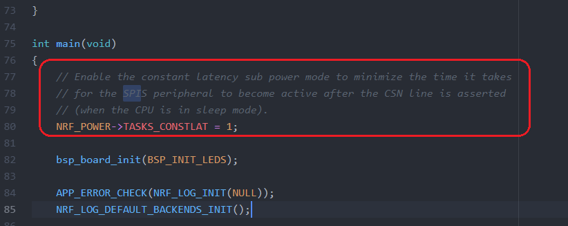
By using the SPI Slave, it should need to enable the Constant Latency mode in order to minimize the time for CS when the MCU is in sleep mode.
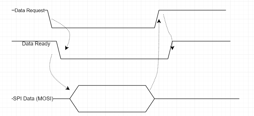
In order to use the NRF52 as SPI slave mode, it needs to add extra GPIO pin in order to data request from slave to master.
For the below configuration, it uses additional 3 GPIO pins to communicate with SPI interface. It can use to wake up the SPI Master / Slave from sleep mode in order to save current consumption.

For example,
Case 1
Master initiatively requests to send data.
Case 2
Slave initiatively requests to send data. Given the master should know how many bytes Slave plans to send.